Typical semiconductor component: Vacuum system (1)
Category: News
Time:2024-12-09
Vacuum System - The Largest Semiconductor Subsystem
Vacuum refers to the state of gas in a given space that is below atmospheric pressure. Vacuum technology is the technology required to create a physical environment below atmospheric pressure, as well as to carry out processes, physical measurements, and scientific experiments in this environment.
Manufacturing semiconductor chips must be done in a vacuum environment to avoid oxidation and contamination, ensuring chip quality and performance.
At normal temperature and pressure, the environment contains a large amount of impurities, making chips susceptible to oxidation and contamination during the semiconductor manufacturing process, which severely affects chip quality and production efficiency.
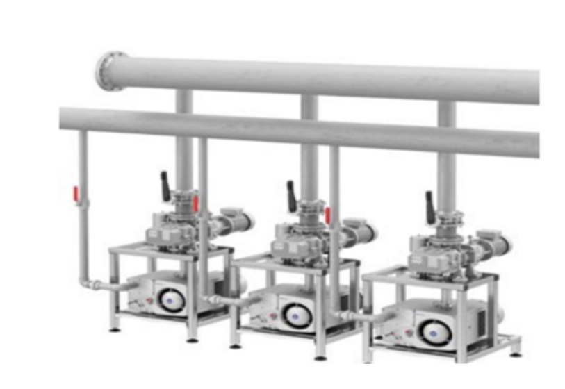
In vacuum technology, vacuum degree is commonly used to measure the thinness of gas in a vacuum state, usually represented by the pressure value of the gas. The higher the pressure value, the lower the vacuum degree; the lower the pressure value, the higher the vacuum degree. A vacuum system consists of components such as vacuum pumps, control systems, gas storage tanks, and piping installations, including many core semiconductor components like molecular pumps, cryopumps, dry pumps, isolation valves, control valves, transfer valves, and O-Ring seals.
Source: Vacuum Technology Equipment Network
| Effects of Achieving Vacuum Conditions | Benefits |
| Clean Environment | Removal of particles, unwanted gases, water vapor, and contaminants |
| Reduction of Molecular Density | Decrease in molecular density within the system |
| Increase in Molecular Collision Distance | Creation of plasma zones required for processes like sputtering and etching in the semiconductor manufacturing industry |
| Acceleration of Reaction Processes | Reduction of the pressure of reaction vapors |
Source: 'Semiconductor Manufacturing Technology' - Michael Quirk
| Vacuum Degree Range | Pressure Range | Main Application Areas |
| Low Vacuum | 10^5Pa-10^2Pa | Using the pressure difference obtained from low vacuum to hold, lift, and transport materials, as well as for dust collection and filtration. |
| Medium Vacuum | 10^2Pa-10^1Pa | Generally used to remove gases or moisture retained or dissolved in materials, manufacture light bulbs, vacuum metallurgy, and serve as thermal insulation. |
| High Vacuum | 10^-1Pa-10^-5Pa | Used in thermal insulation, electrical insulation, and to avoid molecular electronic ion collisions. |
| Ultra High Vacuum | <10^-5Pa | Commonly used in research on controllable thermonuclear fusion, the production of time reference hydrogen molecular mirrors, and research in surface physics and surface chemistry. |
Source: Maderbao Vacuum Equipment Group, Zhongke Instrument Prospectus
Keywords: Typical semiconductor component: Vacuum system (1)
RELATED INFORMATION
Company Information
Industry Information
-
FFKM Perfluoroether O-Rings: Why Are They So Expensive?
Time:2026-06-11
-
Semiconductor commonly used parts - perfluoro O-ring (Dupont/GT...)
Time:2025-05-28
-
Standard requirements for high-performance perfluoroelastomer seals
Time:2025-05-13
-
SEMICON 2025 - Hongxin Fluoroethers Invites You to View the World's Largest Semiconductor Exhibition!
Time:2025-03-19
-
"2024 to 2030 Deep Analysis and Development Trend Research Forecast Report on China's Perfluoroether Rubber (FFKM) Industry"
Time:2025-01-17
-
Dry etching and wet etching in semiconductor etching film processes are suitable for different specific scenarios. 1. **Dry Etching**: - **Applications**: Typically used for high-resolution patterning, such as in the fabrication of integrated circuits (ICs) and microelectromechanical systems (MEMS). - **Advantages**: Provides better control over etching profiles, allows for anisotropic etching (vertical etching), and is suitable for etching complex geometries. - **Common Techniques**: Reactive Ion Etching (RIE), Deep Reactive Ion Etching (DRIE), and Plasma Etching. 2. **Wet Etching**: - **Applications**: Often used for bulk material removal, cleaning, and in processes where isotropic etching is acceptable, such as in the fabrication of certain types of sensors and optical devices. - **Advantages**: Generally simpler and less expensive than dry etching, and can be more effective for certain materials. - **Common Techniques**: Acid or alkaline solutions are used to etch materials like silicon, silicon dioxide, and metals. In summary, dry etching is preferred for applications requiring precision and complex patterns, while wet etching is suitable for simpler tasks and bulk material processing.
Time:2025-01-08
-
Typical semiconductor component: Vacuum system (1)
Time:2024-12-09
-
How to buy the right size perfluoroether rubber special-shaped seal ring
Time:2024-03-28
-
Maintenance methods and precautions of perfluorinated ether rubber special-shaped sealing ring
Time:2024-03-20
-
Analysis of Application Prospect of Perfluorinated Ether O-ring in Aerospace Field
Time:2024-02-14
-
Application and Development of Special-shaped Seal Ring in Oil Exploitation Technology
Time:2023-12-26
-
About the installation knowledge of perfluorinated ether O-ring
Time:2023-12-21
-
Where are perfluorinated ether O-rings widely used?
Time:2023-11-06
-
What is the difference between perfluoro rubber and perfluoro ether
Time:2023-09-14
-
The difference between perfluoroelastomer flange center ring and ordinary flange center ring
Time:2023-07-17
-
What is perfluoroether rubber? What are the characteristics of perfluoroether sealing products?
Time:2023-07-11

Website QR Code
COPYRIGHT © 2024 HONGXIN FFKM TECHNOLOGY CO., LTD. ALL RIGHT RESERVED. POWER BY: 300.CN